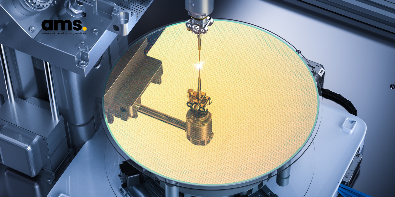
What Is the Optimal Solution for Semiconductor Wafer Polishing?
AMS offers semiconductor wafer polishing solutions tailored for manufacturers seeking to enhance efficiency, reduce costs, and adopt sustainable practices by minimizing chemical waste. In a highly competitive market, manufacturers often face similar challenges—so what are the best strategies to optimize production segments and gain a competitive edge? Specifically, in niche markets like semiconductor wafer manufacturing, how does polishing optimization contribute to economic benefits? Explore the details in the article below!

1. Market Overview of Semiconductor Wafer Grinding and Polishing Equipment
A. Global Market Growth Drivers
The semiconductor wafer grinding and polishing equipment market is projected to experience positive growth, driven by the increasing demand in the electronics sector. According to market analysis by Mordor Intelligence, the rising need for MEMS, microchip manufacturing, optics, and compound semiconductors is accelerating planarization processes in semiconductor devices. Given the current market landscape, where nearly all electronic devices—including laptops, smartphones, and computers—rely on silicon ICs and semiconductor-based packaging, the demand for advanced grinding and polishing equipment continues to rise.
Beyond the electronics industry, the growth of the electric vehicle (EV) sector is also fueling semiconductor wafer demand, particularly for power semiconductor ICs used in automotive applications. According to the U.S. Department of Energy (DoE), EV sales surged by 85% from 2020 to 2021, while plug-in hybrid electric vehicle (PHEV) sales more than doubled in 2021, increasing by 138% year-over-year. Semiconductors play a critical role in EV systems, enabling key components of the electrified drivetrain, such as chargers, DC-DC converters, and traction inverters.
B. Market Growth Drivers in Vietnam
Vietnam is also part of the global growth trend, with various manufacturing sectors driving the expansion of the wafer grinding and polishing industry. The Vietnamese electric vehicle (EV) market is estimated to reach $2.93 billion by 2025 and is projected to grow to $6.69 billion by 2030, with a compound annual growth rate (CAGR) of 18% during the forecast period (2025-2030).
Meanwhile, Vietnam's semiconductor market is expected to reach $7.01 billion by 2028, according to the Global Semiconductor Alliance (SEMI). Additionally, Vietnam's semiconductor industry development strategy aims to achieve an annual revenue scale of over $25 billion between 2024 and 2030. These market projections present significant opportunities for the wafer grinding and polishing sector.

2. How Is a Silicon Wafer Polished?
A wafer is a thin slice of silicon, approximately 30 mil (0.76 mm) thick, cut from a cylindrical silicon ingot. This component is used as a substrate material for manufacturing integrated circuits (ICs) by embedding different materials onto its surface to create circuits with various properties.
To produce a semiconductor wafer, silicon must be polished to achieve a flat, smooth, and mirror-like surface finish. There are two main polishing methods: Chemical Mechanical Polishing (CMP) and Physical Vapor Deposition (PVD).
-
CMP involves using a chemical solution to remove material from the wafer surface.
-
PVD uses a physical process to deposit thin films onto the wafer surface.
Manufacturers typically prefer CMP for polishing silicon wafers, as it generally provides higher precision and surface quality.
>> See more: Applications and Classification of Hyperion Polishing Compounds
3. CMP and the Challenges Faced by Wafer Manufacturers
Chemical Mechanical Polishing (CMP) is a process that combines chemical reactions and mechanical polishing to remove material from the surface of a semiconductor wafer. The chemical component of CMP reacts with the wafer surface, while the mechanical component removes material through physical abrasion. CMP is a highly controlled process, where variations in the composition of the chemical slurry and the type of polishing pad can result in different material removal rates.
With this process, manufacturers aim to achieve uniform material removal across the wafer surface while minimizing surface damage. However, silicon carbide (SiC), known for its extreme hardness and brittleness, presents significant challenges. Manufacturers must find ways to enhance processing efficiency, optimize polishing techniques, and prevent surface damage.
If incompatible materials or excessive force are applied during processing, wafers can develop cracks, defects, and chipping, potentially leading to substantial revenue losses.
Additionally, CMP is a cost-intensive step for wafer manufacturers, accounting for up to 50% of the total wafer finishing cost due to chemical waste and polishing time.
4. The Impact of Diamond in Enhancing SiC Wafer Processing Efficiency
Diamond, the hardest material in the world, plays a crucial role in SiC wafer processing from the initial stages. It is used to remove SiC material before the final polishing steps, a critical phase that eliminates surface defects in SiC wafers. However, this process is time-sensitive and often becomes a bottleneck, impacting production efficiency.
Understanding this challenge, Hyperion has developed an ultra-fine diamond slurry featuring micro-etched diamond surfaces. With an enhanced surface structure that increases cutting points, this ultra-fine slurry significantly accelerates SiC wafer polishing, reducing the time required to produce an epi-ready wafer. By dramatically improving processing efficiency while achieving exceptional surface quality in later SiC processing stages, Hyperion's ultra-fine diamond presents a compelling alternative to traditional, lengthy CMP steps.
Through the development of Quantis™ Polishing Slurries, a unique range of micro-etched diamond slurries with extremely high material removal rates, Hyperion optimizes the final polishing process for silicon carbide. Quantis™ ensures high-quality epitaxial layers that meet the strict standards of the semiconductor industry while simultaneously reducing surface roughness and shortening the polishing time of ultra-hard substrate wafers. By adopting a two-step polishing process with Quantis™ Polishing Slurries, wafer manufacturers can cut production costs by up to 70%, making their operations significantly more cost-effective.
5. Why Choose AMS for Your Polishing Solution?
At AMS, we take pride in our two-decade journey in the precision engineering market. Over the years, we have been a trusted partner to leading manufacturers across various industries in Vietnam, including mold-making, plastics, automotive, gas, and consumer electronics.
As Vietnam's wafer and semiconductor manufacturing sector continues to grow, we firmly believe that our mission extends beyond any single industry. AMS is committed to expanding our reach, bringing cutting-edge polishing solutions and globally recognized brands to semiconductor manufacturers in Vietnam.
Beyond offering premium polishing solutions, AMS provides a seamless purchasing experience with flexible procurement policies, transparent transactions, and streamlined procedures. Choosing AMS means choosing efficiency, reliability, and expertise—we stand by our commitment to delivering the best polishing solutions for your needs!
6. Conclusion
The optimal polishing solution for semiconductor wafers is developed by Hyperion and distributed by AMS Vietnam. Thank you for taking the time to read this article - contact AMS today for inquiries, expert consultation, or further assistance!
AMS Company, Ltd.243/9/10D To Hien Thanh, Ward 13, District 10
Hot line: 028.3868 3738/3903 - Fax: 028.3868 3797
